| Telefon: |
+420 54114 2707 |
| E-mail: |
|
| Kancelář: |
|
| Telefon: |
+420 54114 2848 |
| E-mail: |
,
|
| Kancelář: |
|
Research areas
-
Fabrication of nanostructures using bottom-up methods
-
Fabrication of nanostructures using top-down methods (nanolithography)
-
Investigation of the functional properties of nanostructures
-
The development of analytical and measurement methods
Main objectives
Fabrication of nanostructures using bottom-up and top-down methods (nanolithography)
Development of methods for the fabrication of nanostructures: planar physical and plasmochemical methods using EBL, UV lithography, FIB, SPM lithography, and imprint technology. MBE, CVD, ALD, PECVD, hybrid methods for selective growths, etc. All the methods developed are utilized directly for fabrication of nanostructures, advanced planar materials and devices.
Investigation of the functional properties of nanostructures
Specification and optimization of the functional properties of nanostructures for nanoelectronics, nanophotonics and (bio)sensing their correlation with geometrical/structural parameters of nanostructures and operational parameters. Novel and unique properties of nanostructures not observable in conventional materials and microstructures open the ways for qualitatively new applications.
Research and development of analytical and measurement methods
Development of techniques and methodologies for microscopy, analysis and metrology of nanomaterials/nanostructures, and for diagnostics of their properties – new techniques of nanometrology by SPM, optical methods, combination of more techniques (SEM, AFM, etc.). This will be used to meet the other objectives of the Advanced Nanotechnologies and Microtechnologies Research Programme and for the characterization of nano- and microstructures generally.
Content of research
Fabrication of nanostructures using bottom-up methods
Fabrication of nanostructures using planar technologies
Research and utilization of phenomena essential for the growth of (ultra)thin films and self-assembling of nanoobjects (nanofibres, nanotubes, nanodots etc.) with specific properties using PVD (MBE, IBAD, magnetron sputtering), CVD, PECVD and (electro)chemical methods. Attention will be paid both to the study of the initial stages of the growth of thin films and nanostructures that are of vital importance for the parameters and properties of the final products (substrate influence, nucleation, diffusion, growth modes, catalytic activity), and to finding relationships between the parameters and the properties of these products. Selective and guided growth of nanostructures on the substrates patterned by lithographic methods.
Research on the fabrication of nanofibres (especially metallic) from electrolytic solutions using e.g. polymeric and alumina matrices and the development of methods of assembling nanofibres using electrophoresis, etc.
Fabrication of nanostructures using top-down methods (nanolithography)
The development of nanolithographic methods by means of electron beam lithography, scanning probe microscopy (e.g. local anodic oxidation), focussed ion beam and their combinations with planar technologies (e.g. selective and guided growth, respectively) for the fabrication of nanostructures with minimum dimensions as close to 10 nm as possible.
-
Fabrication of nanoelements and nanodevices (quantum point contacts, rings and dots, SETs, spintronics systems, etc.)
-
Fabrication of ordered metallic nanoparticles, elements and systems (plasmonics, resonance plasmonic antennas, etc.)
-
Fabrication of ordered dielectric and semiconductor nanodots and nanowires (photonics, optoelectronics, bioactive surfaces)
-
Fabrication of metallic nanoelectrodes for making contacts to molecular nanostructures and nanoelements
-
Fabrication of novel masks (e.g. from SAM), the application of self-assembling and electrochemical methods

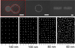
Selective deposition of Au coloids
Negative (top) and positive (bottom) deposition of 20 nm gold nanoparticles after patterning Si substrate with Ga ion beam and immersion in the 3mM HF-modified Au colloidal solution.
Investigation of the functional properties of nanostructures
The main goal is to find correlations between the properties and the geometrical and structural parameters of nanostructures and to use this knowledge for feedback in the technology of their preparation and for various applications.
Magnetic nanostructures
The fabrication of magnetic 2D-0D ordered nanostructures and ultrathin-layered structures utilizing the combination of 3D metals and nonmagnetic materials. An experimental and theoretical study of magnetic anisotropy, transport properties (e.g. GMR, TMR) and the dynamics of domain walls and vortexes for applications in magnetic recording, sensing and spintronics.

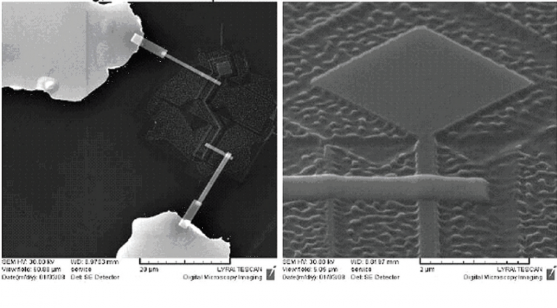
Spin valve nanowires
Nanostructures for plasmonics
The fabrication and study of the properties of metallic nanostructures and microstructures suitable for plasmonics. Research on the generation, detection and application of surface plasmon polaritons. Simulation and experimental verification of localized surface resonances (localized surface plasmons) on metallic nanoparticles, nanowires and nano/micro antennas. The influence of dielectric materials (spacers) between metallic components of plasmonic structures. Applications in micro and nanosensors (including biosensors).

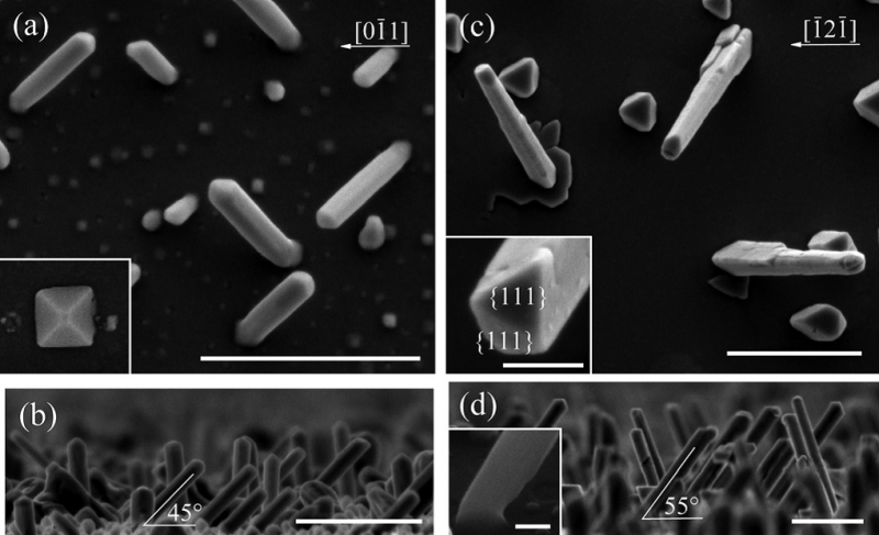
Top and side views of Ge NWs grown on Ge(100) and Ge(111) substrates.
The scale bars represent 1 mm, in insets 200 nm.
Ultrathin films and nanostructures of wide-band gap semiconductors
The fabrication of semiconductor nitride ultrathin films and nanostructures (GaN, AlN) at low and medium temperatures. A study of their electronic structures. The electric transport properties and optoelectronic properties of 0D nanostructures.
Research group SITE
CURRENT RESEARCH INFRASTRUCTURE
The experimental facilities of the group are mainly located in clean rooms (class < 100 000). They include the following equipment:
Dual ion beam HV apparatus for ion-beam assisted deposition and ion-beam etching; complex UHV apparatus for deposition and in situ analysis of ultrathin films with four effusion cells for molecular beam deposition, a hyperthermal ion-beam source for direct ion beam deposition, and surface analytical techniques (SIMS, TOF-LEIS, XPS, TDS, LEED, RHEED, spectroscopic ellipsometry); two commercial scanning probe microscopes (AutoProbe Veeco, NT-MDT Ntegra) providing various modes such as AFM, LFM, conductive AFM, EFM, Kelvin probe, nanolithography mode and in case of NT-MDT microscope also a near field mode (SNOM) providing illumination and collection operational regimes both in reflection or transmission (inverted microscope) measuring schemes; FIB system (Tescan Mira), microreflection spectrometer; a setup for magnetooptical Kerr effect, etc. Other instruments such as standard and confocal optical microscopes and a scanning electron microscope with a lithographic option (Tescan – Vega) are available in the labs outside of the clean rooms.


