+420 54114 9207 |
  nano@ceitec.vutbr.cz
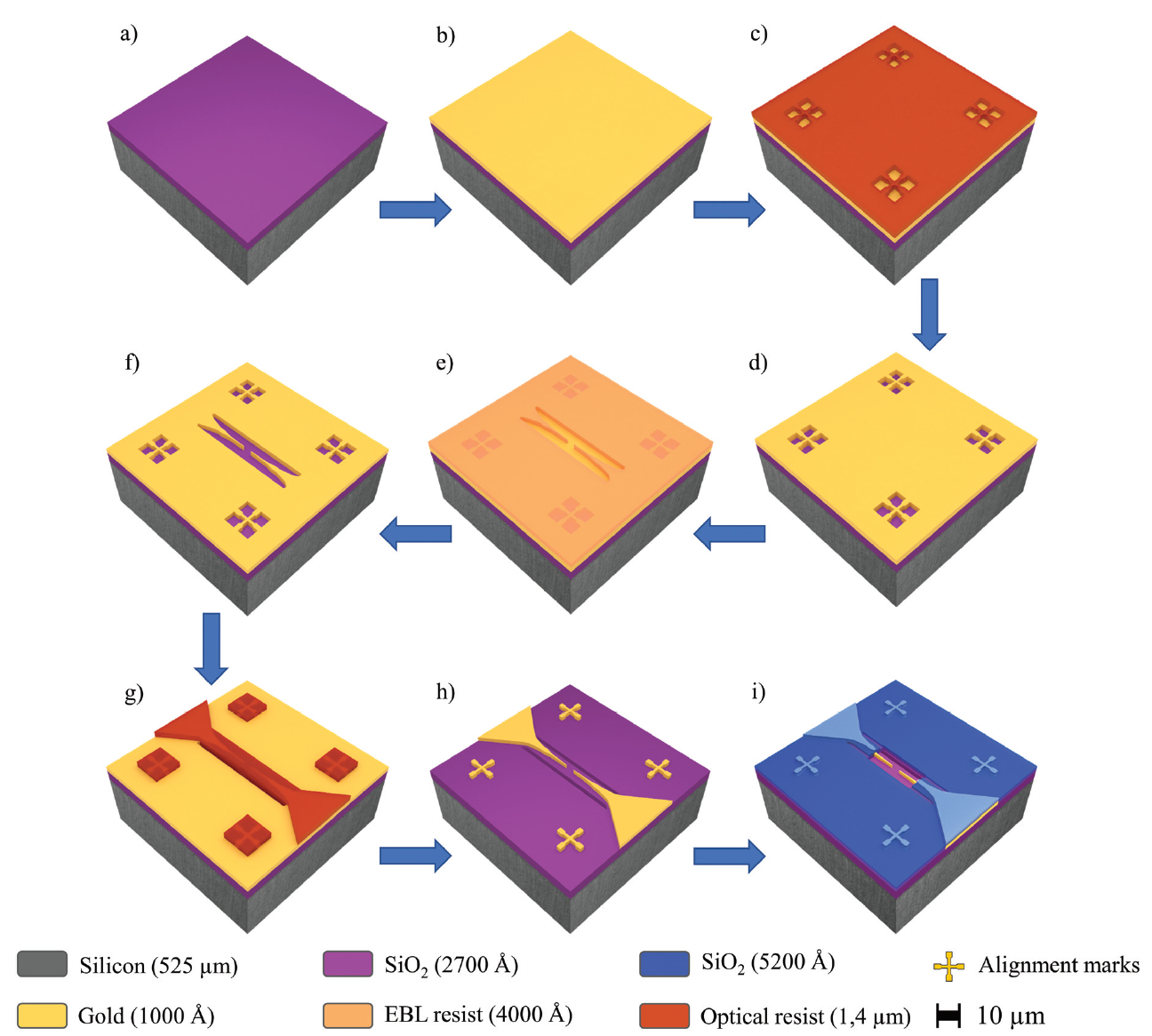
Single nanowire gas sensing devices provide better sensitivity, stability and better selectivity than bulk materials thanks to the presence of specific crystal facets offering well-defined surfaces.
On the nanoelectrode arrays featuring single nanowires fabricated at CEITEC Nano Core facility O. Chmela and coworkers showed reproducible gas sensing performance.
Employing combination of electron beam and optical lithography authors were able to manufacture platform in which single nanowires can be easily integrated by dielectrophoresis. These finding present the important step in fabrication of multifunctional sensor arrays.
O. Chmela, J. Sadílek, G. Domènech-Gil, J. Samà, J. Somer, R. Mohan, A. Romano-Rodriguez, J. Hubálek, S. Vallejos: Selectively arranged single-wire based nanosensor array systems for gas monitoring. Nanoscale 2018, 10, 9087.
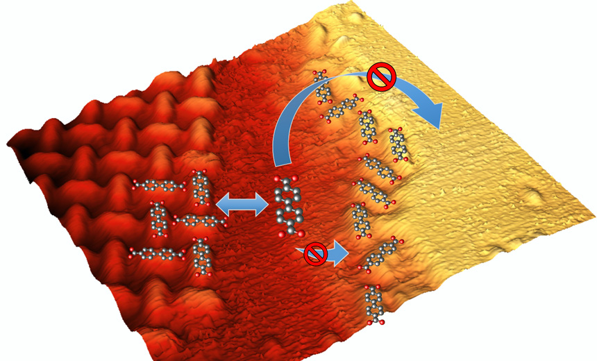
Fabrication of molecular films with a defined functionality requires the full understanding of the underlying physics. However, several molecular systems show an unusual growth behavior, for example, biphenyl dicarboxylic acid deposited on copper substrate simultaneously displays strong interaction with substrate and low interaction with substrate step edges.
A direct visualization of the system at molecular level provided by the complex UHV system of CEITEC Nano allows explaining the observed unusual growth.
Employing scanning tunneling microscopy, Lukáš Kormoš with his colleagues revealed that the strong molecular substrate interaction is even more pronounced at substrate step edges. This results in the formation of a molecular row decorating step edge, which prevents the attachment of the any further molecules there. On a mesoscopic level this is expressed as molecular repulsion from the step edges.
L. Kormoš, P. Procházka, T. Šikola, J. Čechal: Molecular Passivation of Substrate Step Edges as Origin of Unusual Growth Behavior of 4,4′-Biphenyl Dicarboxylic Acid on Cu(001), J. Phys. Chem. C 2018, 122, 2815.
Passivation of metals using protective coatings is a widespread technology and represents a huge market that generates billions of US dollars every year. 2D material offer the possibility to provide efficient protection against environment while the properties of the metal being protected are retained.
The high spatial resolution chemical analysis performed at CEITEC Nano Core facility provides insight in the mechanism of surface passivation against water and air oxidation.
The results revealed that when exposed to H2O2, a monolayer h-BN film is as inefficient as graphene as a protective coating. In contrary, 5–7 layers-thick h-BN film showed good protection, probably because of the higher resistance to transverse electron transfer from the metal to the electrolyte.
L. Jiang, N. Xiao, B. Wang, E. Grustan-Gutierrez, X. Jing, P. Bábor, M. Kolíbal, G. Lu, T. Wu, H. Wang, F. Hui, Y. Shi, B. Song, X. Xie, M. Lanza: High-resolution characterization of hexagonal boron nitride coatings exposed to aqueous and air oxidative environments, Nano Res. 2017, 10, 2046.
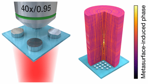
Phase-altering metasurfaces comprise a new class of artificial materials that allow to manipulate the wavefront of passing light and thus provide unprecedented functionalities in optics and nanophotonics.
On the metallic nanostructures fabricated at CEITEC Nano Core facility two CEITEC groups were able to perform quantitative 3D phase retrieval.
Using coherence-controlled holographic microscopy authors can obtain information about the phase of light from the whole field of view of an optical microscope in a single measurement. Quantitative 3D phase map of fabricated plasmonic zone plate shows functional phase lens with thickness below 50 nm.
J. Babocký, A. Křížová, L. Štrbková, L. Kejík, F. Ligmajer, M. Hrtoň, P. Dvořák, M. Týč, J. Čolláková, V. Křápek, R. Kalousek, R. Chmelík, T. Šikola: Quantitative 3D Phase Imaging of Plasmonic Metasurfaces, ACS Photonics 2017, 4, 1389.
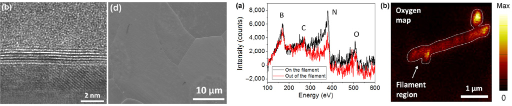
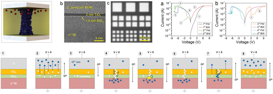
Resistive random access memories (RRAM) have emerged as the flagship element allowing future massive data storage due to their excellent performance and easy fabrication. To fulfill the information storage needs of modern societies, the performance of electronic nonvolatile memories (NVMs) should be continuously improved.
The devices fabricated at CEITEC Nano Core facility show the way how to further extend the performance of RRAMs.
Ti/2-nm-TiO2/1.5-nm-SiOX/n++Si memristors exhibit unprecedented I–V characteristics with double hysteresis. This behavior is related to the coexistence of filamentary and distributed resistive switching. The simplicity of our design and the good compatibility of all the materials used (Ti, TiO2, SiOX, and n++Si), with the silicon technology give promise that these findings will be quickly implemented in real devices.
N. Xiao, M. A. Villena, B. Yuan, S. Chen, B. Wang, M. Eliáš, Y. Shi, F. Hui, X. Jing, A. Scheuermann, K. Tang, P. C. McIntyre, M. Lanza: Resistive Random Access Memory Cells with a Bilayer TiO2/SiOX Insulating Stack for Simultaneous Filamentary and Distributed Resistive Switching, Adv. Funct. Mater. 2017, 27, 1700384.
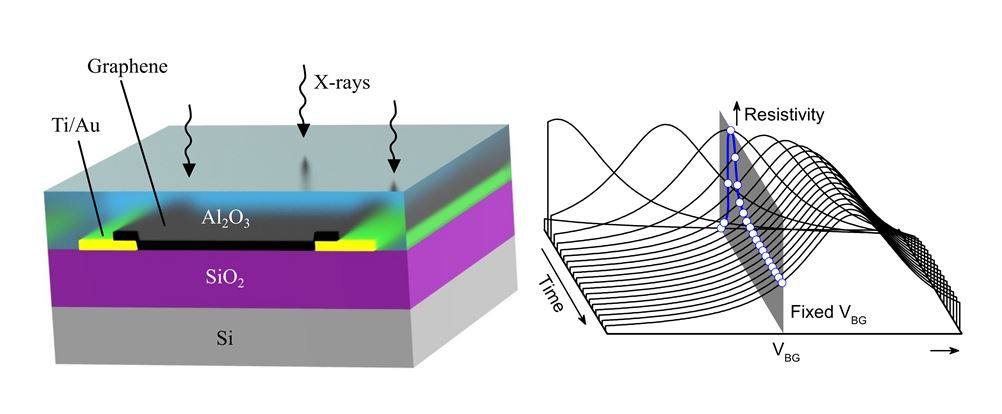
Graphene is a zero bandgap semiconductor. In this respect, applying external electric field it is possible to control the charge carrier type (negative or positive) and concertation in graphene, therefore to change it transport properties (e.g. resistance). This usually requires several fabrication steps, i.e. fabrication of graphene effect transistor device.
Employing the graphene devices fabricated in CEITEC Nano Core Facility Pavel Procházka and his colleagues have found that the graphene can be doped using the X-ray radiation.
In this way, the graphene properties can be remotely defined without need for any contacts. Moreover, results of the study define the framework for correct X-ray characterization of graphene and can be developed into graphene radiation sensors.
P. Procházka, D. Mareček, Z. Lišková, J. Čechal, T. Šikola: X-ray induced electrostatic graphene doping via defect charging in gate dielectric, Sci. Rep. 7 (2017), 563.
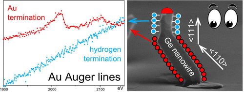
Mira Kolíbal used NanoSAM at CEITEC Nano to reveal the essential role of atomic hydrogen in determining the growth direction of Ge nanowires with an Au catalyst.
M. Kolíbal, T. Pejchal, T. Vystavěl, T. Šikola: The synergic effect of atomic hydrogen adsorption and catalyst spreading on Ge nanowire growth orientation and kinking, Nano Lett. 16 (8), (2016), 4880–4886.
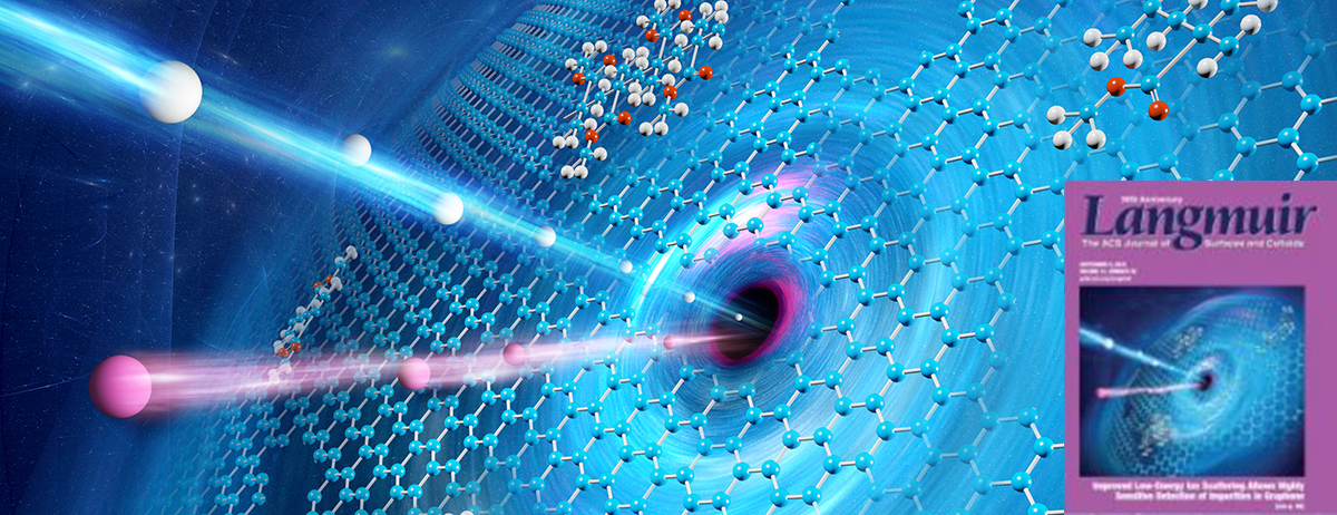
The paper resulting from work on TOF-SIMS QTAC by Stan Průša, Pavel Procházka, Petr Bábor, Tomáš Šikola and their coworkers was chosen by Langmuir editor as the Editors choice!
S. Průša, P. Procházka, P. Bábor, T. Šikola, R. ter Veen, M. Fartmann, T. Grehl , P. Brüner, D. Roth, P. Bauer, H. H. Brongersm: Highly Sensitive Detection of Surface and Intercalated Impurities in Graphene by LEIS, Langmuir 31 (2015), 9628.