+420 54114 9207 |
  nano@ceitec.vutbr.cz
 Nanolithography
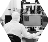
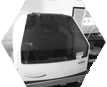
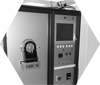
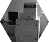
 | E-beam writer RAITH150 Two (RAITH)The Raith 150 Two is a high resolution low voltage electron lithography (EBL) and metrology system. It is suitable for research and development of MEMS, micro and nanoelectronic, plasmonic, photonic systems and integrated optical devices. |
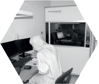
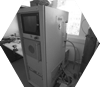
 | Scanning Electron Microscope/E-beam writer TESCAN MIRA3/RAITH LIS (MIRA)A scanning electron microscope equipped with laser interferometry stage capable of working with samples up to 50x50 mm2. Overlay and stitching accuracy below 100 nm, linewidth below 20 nm. |
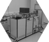
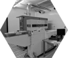
 | UV Direct Write Laser system HEIDELBERG DWL 66-fs (DWL)The DWL 66FS laser lithography system is a high resolution pattern generator for low volume mask making and direct writing. The capabilities and flexibility of this system allows the use of this research tool in MEMS, BioMEMS, Micro Optics, ASICs, Micro Fluidics, Sensors, CGHs, and all other applications that require microstructures. |
 | Spincoater Laurell WS-650-23B (LAURELL)The Laurell WS-650-23 B spin coater is compact and packed with advanced features. This 650-series coater system will accommodate up to ø150mm wafers and 5" × 5" (127mm × 127mm) substrates, and features a maximum rotational speed of 12,000 RPM (based on a ø100mm silicon wafer). |
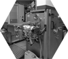
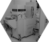
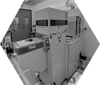
| Mask Aligner SÜSS MicroTec MA8 (SUSS-MA8)The Süss MicroTec MA8 is a standard UV lithography tool for exposing wafers through mask. Exposure can be carried out in proximity mode or in contact mode. The MA8 is equipped with top side optical microscopes and bottom side microscopes, so alignment is possible from both sides of the wafer. |
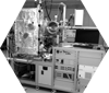
 | Coating and development system SÜSS MicroTec RCD8 (SUSS-RCD8)The RCD8 coat and develop platform is equipped with a basic manual spin coater and a GYRSET® enhanced coater and puddle developer tool. It can handle small pieces as well as standard wafers up to 200 mm and therefore is ideal for daily R&D work up to small scale production. |
| Lithographic wetbench for coating (SUSS-WETBENCH)The wetbench provides a complete basic setup for substrate coating. It consists of the built-in spin-coater LabSpin 6 for manual resist dispense, two hot plate modules HP8, and one vapour primer VP8 for HMDS coating (adhesion promoter). |
 | Mechanical profilometer Bruker Dektak XT (DEKTAK)The Dektak stylus surface profiler is an advanced thin and thick film step height measurement tool. In addition to profiling surface topography and waviness, the Dektak system measures roughness in the nanometer range. |
 | Resist stripper Diener NANO Plasma cleaner (DIENER)The Diener NANO Plasma Cleaner with microwave generator can be used for resist stripping. Microwave plasma is ideal for most resist removal in modern device fabrication. |
 | Spectroscopic reflectometer Ocean Optics NanoCalc 2000 (NANOCALC)Multilayers characterization, resist thickness measurement mainly. Interval of measure film thickness from 10 nm up to 100 µm. |
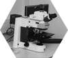 | Optical microscope Zeiss Axio Imager A2 (ZEISS-A2)Microscope Zeiss Axio Imager A2 for control of lithography processes in reflected-light, bright field and dark field. Equipped with PC interface. |
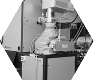
Etching & Deposition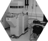 | Deep reactive ion etching of Si-based materials, Oxford Instruments Plasma Technology PlasmaPro 100 (DRIE)Deep reactive-ion etching (DRIE) is a highly anisotropic etch process used to create deep penetration, steep-sided holes and trenches in wafers/substrates, typically with high aspect ratios. |
 | Experimental PECVDThe Experimental plasma enhanced CVD reactor is constructed for diagnostics of plasmachemical processes in capacitively coupled radio frequency (RF) discharges (13.56 MHz). It is possible to measure a delivered RF power, investigate presence of plasma-excited species by optical emission spectroscopy, obtain information about energy and flux of ions impinging on the substrate RF electrode, and measure mass and ion energy spectra of plasma phase particles. |
 | High temperature plasma enhanced chemical vapour deposition system on C-based materials, Oxford Instruments Plasma Technology NanoFab (PECVD-NANOFAB)Chemical vapour deposition system reaching very high deposition temperatures dedicated to the deposition of carbon nanomaterials, possibilities of plasma enhancement by discharges of different frequency (including their regular switching). |
 | Ion beam etching Scia Systems Coat 200 (SCIA SYSTEMS)The physical vapor deposition method allows thin films to be etched by the use of broad beams of positively charged ions in a high vacuum system. The system is equipped with SIMS spectrometer for precise end-point detection. |
 | Magnetron sputtering system BESTEC (MAGNETRON)The system consists of a sputter deposition chamber with 8 magnetrons in sputter up configuration. The lid flange of the sputtering chamber is sealed with double viton O-rings and differentially pumped. |
 | Rapid thermal annealing Xerion XREACT/1 250°C (XERION)The heating sources for the XREACT radiation furnaces are halogen lamps or short arc lamps. Heating rates up to 150 k/s are possible. In our Rapid Thermal Processing (RTP) systems wafers can be annealed. As components of testing machines, the radiation furnaces are very small and are especially used for thermo mechanic fatigue (TMF) tests. |
 | Metal organic chemical vapor deposition (MOCVD)System for deposition of thin layers of metal oxides on a horizontally oriented wafer/sample inside a cylindric steel reactor, with higher growth speed and lower control of layer thickness than a related ALD technique. |
 | Atmospheric Pressure chemical vapor deposition (APCVD)System for a precisely controlled growth of oxides on silicon wafers in horizontal quartz tubes with soft-loading placement of boats holding up to 50 wafers in one run. |
Low Pressure chemical vapor deposition – amorphous Si (LPCVD-polySi)This position within the LPCVD system is dedicated to growth of amorphous silicon on Si wafers, using silane (SiH4) as a precursor in LPCVD process. | |
Low Pressure chemical vapor deposition – Si nitrides (LPCVD-SiN)This position within the LPCVD system is dedicated to growth of silicon nitrides of different stechiometry on Si wafers, using dichlorosilane (SiCl2H2) and ammonia (NH3) as precursors in LPCVD process. | |
 | Plasma Enhanced CVD of Si-based materials, Oxford Instruments Plasma Technology PlasmaPro 100 (PECVD)Plasma enhanced chemical vapour deposition using chemically reactive plasma for deposition of silicon based materials. |
 | RIE by Fluorine Chemistry and PECVD of hard C-based films, Oxford PlasmaPro NGP 80 (RIE-FLUORINE)Thin film deposition by plasma enhanced chemical vapour deposition. Etching of silicon and metals by reactive ion etching. |
 | RIE by Chlorine Chemistry, Oxford Instruments Plasma Technology PlasmaPro 100 (RIE-CHLORINE)Reactive-ion etching (RIE) is an etching technology used in microfabrication. RIE is a type of dry etching which has different characteristics than wet etching. RIE uses chemically reactive plasma to remove material deposited on wafers. |
 | Electron beam evaporator BESTEC (EVAPORATOR)Thin film deposition by electron beam evaporation. |
 | Atomic layer deposition system, Ultratech/CambridgeNanoTech Fiji 200 (ALD)Atomic Layer Deposition is a deposition technique for very thin layers with the thickness control down to a single atomic layer. It belongs to the CVD techniques family. |
 | Ion-Beam Sputter Deposition System BESTEC (KAUFMAN)Suitable for Ion-beam sputter deposition, Ion-beam assisted deposition, reactive sputter deposition with nitrogen and in-situ initial/continual substrate (pre-)cleaning. |
SCS Parylene Deposition System (PARYLENE)For Parylene laboratory research, applications developement and testing, the SCS Labcoater 2 Parylene Deposition System (PDS 2010) performs reliable and repeatable application of SCS Parylene conformal coatings. | |
XeF2 etching system (XeF2)XeF2 etchining system is designed to expose samples to xenon difluoride gas (XeF2) in a cyclic mode in which the etch chamber is repeatedly filled with XeF2 gas and pumped out again. The main advantage of XeF2 etching system in comparism to other silicon etchants is in high selectivity to silicon with respect to aluminum, photoresist, and silicon dioxide. Since this technique etch silicon isotropic, large structures can be undercut. |
Packaging | Laser dicer, Oxford Lasers A-Series (LASERDICER)These laser micromachining systems are designed as versatile R&D, process development or pilot production systems. |
| Wire bonder TPT HB 16 (WIREBONDER)Wire bonding is a micro-welding technique for electrical interconnection of the sample substrate structures and semiconductor chip thin metallic layers. Contact between the sample surface and pure gold, alloyed aluminium or copper wire is provided by three main methods: ultrasonic, thermocompression and thermosonic bonding. |
Semiautomatic dicing saw ESEC 8003 (DICING-SAW)A precision machine for cuting semiconductor wafers into individual chips or dice. |
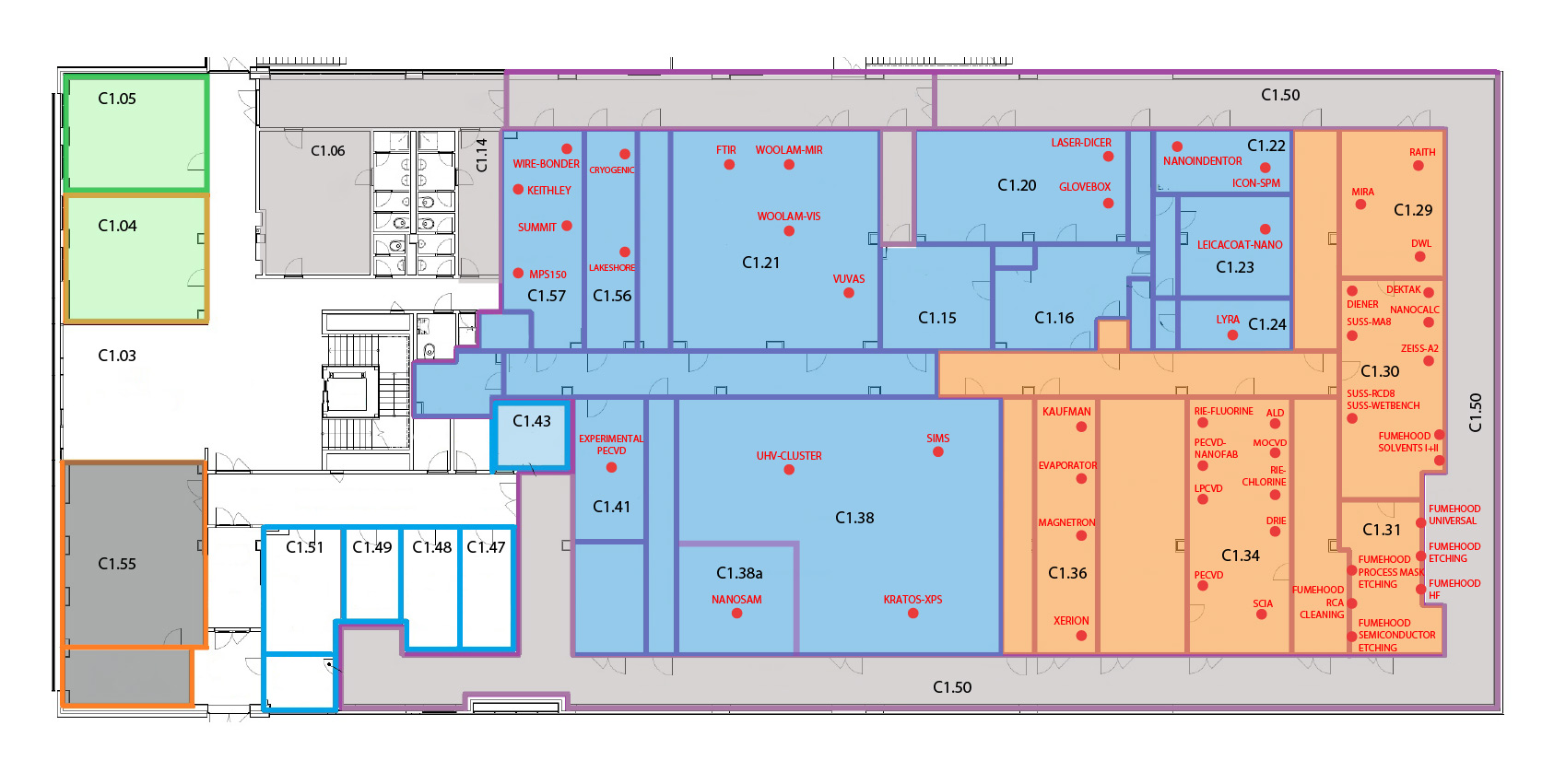
Floorplan and Equipment placement